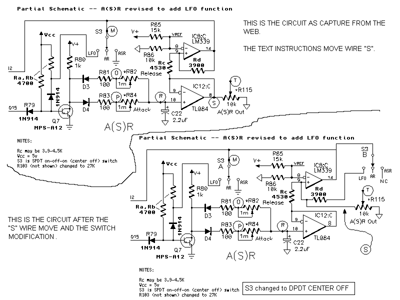
ASR Modification to Provide VCF LFOSee the drawing below for schematic details. Note, Scott Rider's page does not show the correct connection for the wire 'S' in his schematic. I modified the drawing to show the actual connection in the lower drawing. The upper schematic is directly from his site. |
|
The text below was copied from Scott Rider's page for this FatMan mod. The above schematic shows the A(S)R circuit as modified for the added LFO function. Notice that the SPST switch S3, which controlled AR/ASR has been replaced with a SPDT Center Off switch. This switch's positions are LFO/AR/ASR when read left to right. Also note the four added resistors Ra, Rb, Rc and Rd. Two other resistors, R85 and R103, will be changed to new values. Resistor R79 will be replaced by a 1N914 diode, and a second 1N914 will be placed between the base of Q7 and the "LFO" lug on switch S3. Finally, Q7 is changed to an NPN Darlington type and Vcc is wired to Ra and Rb.
Additional parts required:
  Resistors:      3.9K, 4.53K, 4.7K (2), 15K, 27K
  Semiconductors: 1N914 diode (2), MPS-A12 NPN Darlington or eqv.
  Hardware:       SPDT or DPDT on-off-on (center off) miniature switch
  Misc:           10" #22 AWG insulated hook-up wire, spaghetti tubing,
Procedure
  1) Change R85 to 15K, change R103 to 27K.
  2) Unsolder wire from point "S" on board.
  3) Remove jumper wire parallel to R85 (between R85 and IC8).
  4) Solder 4.53K 1% (or any value 3.9K-4.5K) in empty jumper location.
  5) Solder wire taken from point "S" to 4.53K resistor, on the end
       closest to R88.
  6) On solder side of board, solder 3.9K resistor between pins 9 and 14
       of IC8.  Point "S" next to pin 9 is convenient for one lead.

  7) Unsolder connections to AR/ASR switch, remove switch.
  8) Mount SPDT (or DPDT) on-off-on (center off) switch.
  9) Reconnect switch wires.
 10) Solder cathode of a 1N914 diode and one end of a 4.7K resistor to
       unused lug of switch (If DPDT, leave one side unused.)  Insulate
       diode and resistor leads if necessary.
 11) Solder 10" length of insulated wire to "+" lead of C33.  It may help
       to first remove C33, attach the wire, then remount it.

 12) Remove Q7, replace with MPS-A12 NPN Darlington.  (Same orientation.)
 13) Remove R79.  If possible, enlarge hole closest to Q7 with a #60 bit.
 14) Mount second 1N914 in location of R79, with the cathode pointing
       away from Q7.  Solder cathode end only.
 15) Mount one end of a second 4.7K resistor into same hole of R79 occupied
       by the anode of the 1N914 just installed.  If the resistor lead won't
       fit, solder it to the diode's anode lead on the component side of the
       board.  In addition, solder the anode of the 1N914 mounted on the
       switch in step 10 to the anode lead of the 1N914 mounted as R79.
       Finally, solder the lead(s) on the solder side of the board.  Dress
       the component leads to avoid touching other circuit points.  Stripped
       insulation or spaghetti tubing is handy here.  (This is probably
       the trickiest step.)

 16) Trim the free end of the wire installed in step 11 to a length suitable
       for soldering to the free ends of the two 4.7K resistors.  Dress the
       resistor leads and then solder.  Insulate this junction if possible.
OperationThe AR/ASR switch is now an LFO/AR/ASR switch, with the LFO function enabled by flipping the switch bat up. AR is the center position; ASR is the lower position. In the LFO mode, the A(S)R Attack and Release controls become a combination of LFO frequency and symmetry control. The frequency range is approx. 0.1Hz (both controls at max.) to 140Hz (both controls at min.) As the Attack and Release controls are varied, they will adjust the cyclic waveform in the sense of a continuously re-triggered AR envelope. The amplitude of the LFO waveform is 5v p-p nominal.
The CircuitHere's how it works: Positive feedback has been added to the comparator stage IC8:c to change it into a Schmitt Trigger. The hysteresis is the peak-to-peak voltage of the LFO and is set by the ratio Rc/Rb. When the switch is in the AR and ASR positions there is little change in the operation of the circuit. The output of the Schmitt (comparator) signals the computer that the peak output has been reached and the computer responds by turning on Q7 to initiate the Release. When the switch is in the ASR position this signal is grounded and since the computer never sees that the peak has been reached, it never turns Q7 on. Except of course when an NOff or 0V NOn is received from MIDI. In the LFO position of the switch the "peak reached" signal from IC8c is routed back so that it turns Q7 on. When the peak is reached the Schmitt output goes high, turns on Q7 and the Release starts. Release continues until the voltage on C22 falls below the lower Schmitt trigger point at which time the output of IC8c goes low, which turns on Q7 - and so on. It is also worth noting that the computer's AR control bit "O15" does not affect the LFO. This bit is activated (dropped low) only once at the beginning of a note, and goes high whenever the AR "peak reached" signal is sensed by the computer on its "I2" line. If the LFO already has the I2 line high when O15 goes low, O15 goes high within a several microseconds (The amount of time it takes for the firmware to see I2 high and react by setting O15 high.) This is far too short a time to affect the time constant of the 2.2uF storage capacitor and attack/release pots, even at their minimum settings. If the LFO has the I2 line low at the time O15 goes low, the AR/LFO is already in the attack/upslope portion of its cycle: the imminent peak of the cycle will, by setting I2 high, cause O15 to go high. Vref, which is produced by the voltage divider R85 and R86, is lowered because otherwise the higher threshold of the Schmitt will be so high that the voltage on C22 never gets there. Vref is set at 3.2 volts, and provides the maximum possible peak-peak voltage from the LFO. Vref, however, also sets the peak value reached by the ADSR. In order to compensate for this new lower peak voltage, the value of R103 (which scales the VCA V/I converter and is not shown here) should be cut. The ADSRs peak value has been reduced to a little less than half it's previous value so 22k or 27k replaces the present 39k. A note about Rc, Rd: These values will determine the peak-to-peak output of the LFO. Since a single comparator is being used to provide the triggering (instead of the more common dual "window" comparator), the ratio of Rd/Rc is unusually small in order to provide the widest possible hysteresis. This in mind, observe that as Rc is decreased, Vp-p will decrease. It is OK to use a 3.9K resistor for Rc; the Vp-p will be about 4.25 volts. Beyond 4.5K, the Schmitt comparator tends to latch up, making 4.53K (a common 1% value) the upper limit. As for Rd, loading effects of the VCF's V-I converter as the A(S)R level control is rotated toward maximum limit this resistor to 3.9K.
|