 I had asked a question on SDIY regarding options in the absence of OTAs for triangle VCOs. Ian Fritz
sent me this URL: TRI VCO which I read with
great interest. After coming to understand the basic concept of his VCO, I decided to see if I could
do something similar with CMOS, or at least partially in CMOS, hence the "semi" in Semi CMOS Triangle VCO.
I had asked a question on SDIY regarding options in the absence of OTAs for triangle VCOs. Ian Fritz
sent me this URL: TRI VCO which I read with
great interest. After coming to understand the basic concept of his VCO, I decided to see if I could
do something similar with CMOS, or at least partially in CMOS, hence the "semi" in Semi CMOS Triangle VCO.
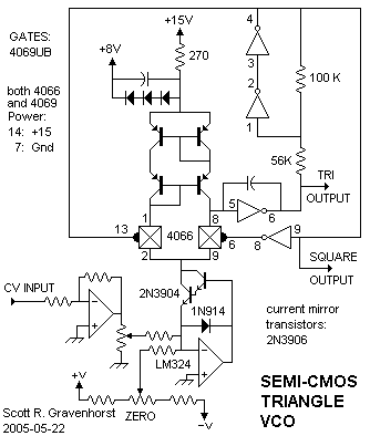
This VCO uses a Wilson current mirror to create the two current sources required for a triangle VCO. When the left switch is closed (the right will be open) the current through the left side of the mirror is copied by the right and sent to the integrator. When the right side is closed (and the left side is open), the current goes from the integrator to the sink. The right side of the mirror passes no appreciable current when the left side's switch is open. The switches, integrator and Schmitt trigger are CMOS. Currently, this is on solderless breadboard and is working. The circuit outputs a triangle waveform above ground (off set is constant) with an amplitude of about 8 volts. For my own use, the offset is not a problem. An expo current sink could be substituted for the linear one that I use. The following things still need attention:
The schematic for this has changed because the current being drawn to or from the 7.5 volt point created by the gate with it's input connected to it's output. During testing, the 4069UB failed. This circuit piece has been replaced by an 8 volt regulator. All in all, I'm not terribly happy with this VCO. Close examination of the ramps yield that they are not perfectly straight. Since straight ramps are required for adequate linearity, I did not do extensive linearity testing. The schematic is here for historical reasons. I may come back to this later, perhaps using less current and a smaller integrating capacitor, but I think the current needs to be 10 times less meaning the capacitor should be 0.001uF. |