 |
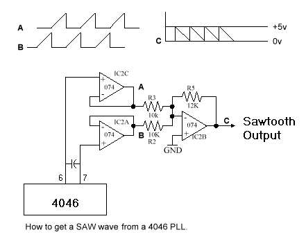
The 4046 employs a flying capacitor VCO. The timing capacitor is in a CMOS transistor bridge. The VCO alternately grounds one side of the capacitor and charges through the transistor on the other side of the bridge. Because of this, the VCO delivers a 50% duty cycle square wave output and the wave forms on pins 6 and 7 are 180 degrees out of phase (see the diagram of waveforms A and B which are taken from pins 6 and 7). While one pin is grounded, we see a ramp on the other pin. Once that ramp is reset, the bridge switches grounding the other side of the capacitor and the other pin has the ramp. If the two pins are voltage followed with a high input impedance opamp such as TL074, the pins' waveforms are recovered and can be added with a third opamp. The sum of the two waveforms is a sawtooth at twice the frequency of the PLL input signal. |